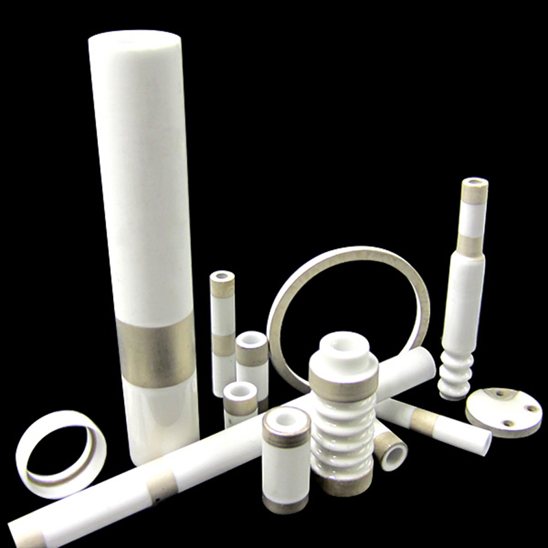
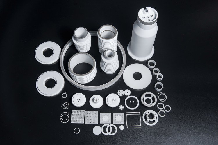
With the continuous advancement of electronic technology, people’s quality of life has improved, and it has also driven the flourishing development of the electronics manufacturing industry. Naturally, this growth has spurred significant advancements in the field of new materials. Precision ceramics are one such area. Among specialized precision ceramics, alumina ceramics have a wide range of applications.
Alumina ceramics can be classified into two types: high-purity and general.
High-purity alumina ceramics refer to ceramic materials with an Al2O3 content of over 99.9%. Due to their high sintering temperature of 1650–1990°C and a transmission wavelength of 1–6 μm, they are commonly used to replace platinum crucibles in molten glass production. They are also utilized for sodium lamp tubes due to their transparency and resistance to alkali metal corrosion. In the electronics industry, they find application as integrated circuit substrates and high-frequency insulation materials.
General alumina ceramics are categorized based on different Al2O3 content, such as 99 ceramics, 95 ceramics, 90 ceramics, and 85 ceramics. Sometimes, those with an Al2O3 content of 80% or 75% are also grouped into the general alumina ceramic series. Among these, 99 alumina ceramics are used in manufacturing high-temperature crucibles, refractory furnace tubes, and special wear-resistant materials like ceramic bearings, seals, and water valve discs. 95 alumina ceramics are primarily used for corrosion-resistant and wear-resistant parts. 85 ceramics, often containing some talc, enhance electrical performance and mechanical strength, enabling bonding with metals like molybdenum, niobium, and tantalum, and are used in electronic vacuum device components.
Alumina ceramics, due to their excellent electrical properties, find extensive applications in the field of electronics and electrical engineering. As a substrate material for electronic devices, surface metallization is crucial as ceramics are insulating materials, requiring surface metallization for electrical conduction. Taget Precision Ceramic Processing specializes in discussing the surface metallization process of alumina ceramics.
Ceramic metallization involves firmly adhering a layer of metal film to the ceramic surface, enabling the bonding of ceramics and metals. A more advanced application involves forming circuits on ceramic surfaces, allowing not only welding but also functioning as conductors for current transmission. Currently, traditional metallization methods include thick-film methods, DBC (Direct Bond Copper) method, DPC (Direct Plated Copper) method, LTCC (Low-Temperature Co-fired Ceramic), HTCC (High-Temperature Co-fired Ceramic), as well as sintering methods like SLID (Solid Liquid Inter Diffusion). Below is a detailed explanation of the advantages and disadvantages of these processes.
1. Thick-Film Method:
Utilizing silk-screen printing to create various circuits, resistors, and capacitors on ceramic bases, this process has extensive applications and can handle substantial currents. However, silk-screen printing’s precision is unsatisfactory, and the bonding between silver paste and ceramics often falls short of expectations. Additionally, the silver paste needs sintering at a specific temperature to solidify. These drawbacks have troubled many industry professionals. The thick-film method results in relatively wide circuit lines, hindering miniaturization in electronic products.
2. DBC (Direct Bond Copper) Method:
Primarily applied in high-power modules, this technique involves thick copper layers capable of carrying large currents, excellent thermal conductivity, high strength, and strong insulation. However, the low reactivity between ceramic substrates and metal materials makes metallization challenging, especially in resolving micro-porosity issues between Al2O3 and copper plates. High sintering temperatures also contribute to high costs, restricting its usage to specific demanding fields.
3. DPC (Direct Plated Copper) Method:
Widely used in the LED field, primarily mastered by Taiwanese manufacturers such as Tong Hsing Electronics with a large shipment volume. Its main advantage lies in high circuit precision, smooth surfaces, suitable for chip-on-board (COB) packaging. Leading international LED manufacturers like Cree and Osram use Tong Hsing’s substrates. The cost is lower than the DBC method. In China, Slitec’s DPC technology has officially entered mass production.
4. LTCC (Low-Temperature Co-fired Ceramic):
This method, using thick-film printing technology to create circuits, results in rough circuit surfaces and imprecise alignment. Multi-layer ceramic stacking during sintering presents challenges regarding shrinkage proportions, limiting its resolution. The widespread application of LTCC ceramic substrates faces significant challenges.
5. HTCC (High-Temperature Co-fired Ceramic):
Due to its extremely high sintering temperature, this method sees minimal usage now and has been essentially replaced by LTCC.
In summary, each traditional method has its drawbacks: high cost, inadequate precision, insufficient process stability, poor adhesion strength, uneven circuit surfaces, and an inability to meet the demands of miniaturization in electronic products. Considering the flaws in these methods, what would a designer do if they needed to design a product meeting these criteria? The Laser Activated Metallization (LAM) process offers a new ceramic wiring technology, also known as Laser Activated Metallization Technology. It involves a surface metallization technique for ceramic three-dimensional components. The LAM process boasts lower costs than DPC, similar circuit density, extremely smooth surfaces, suitability for chip-on-board technology, high adhesion strength, a short and stable process, and the ability to perform wiring on any complex-shaped product, not just limited to flat surfaces.